Skip to content
Home
About Us
Contact Us
Menu
Home
About Us
Contact Us
Category: Material
Application Of Heavy Copper PCB
What To Look For In Biodegradable Sterilization Wraps
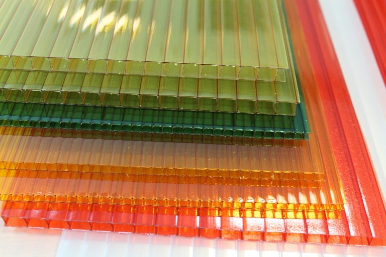
Benefits Of Hard Plastic Sheets
Acrylic Plastic Sheets Are A Perfect Option For Variety Of Applications
No posts found